3 Key Facts About Ball Grid Array Technology

Ball grid array technology has revolutionized modern electronics with its innovative design and functionality. By utilizing solder balls on the underside of the package, it achieves higher input/output density and a smaller footprint compared to traditional packaging methods. This approach enhances electrical performance through shorter paths and ensures efficient heat dissipation. The flexibility of this technology allows for faster and more reliable assembly processes, making it a preferred choice in high-end semiconductor designs. North America, particularly the United States, plays a pivotal role in driving advancements in this field, fostering substantial growth in the global market.
Key Takeaways
BGA technology enhances electrical performance by reducing signal distortion through shorter electrical paths, making it ideal for high-speed applications.
The compact design of BGA packages allows for higher input/output density, enabling the development of smaller, more powerful electronic devices.
BGA excels in thermal management, ensuring efficient heat dissipation which is crucial for maintaining reliability in high-power applications.
Automated assembly processes benefit from BGA's design, leading to improved production efficiency and lower assembly failure rates.
While BGA offers numerous advantages, it requires specialized inspection techniques due to the concealed nature of its solder joints, highlighting the need for advanced quality control.
What is Ball Grid Array Technology?

Definition of Ball Grid Array
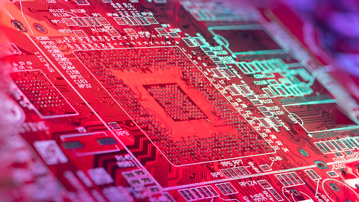
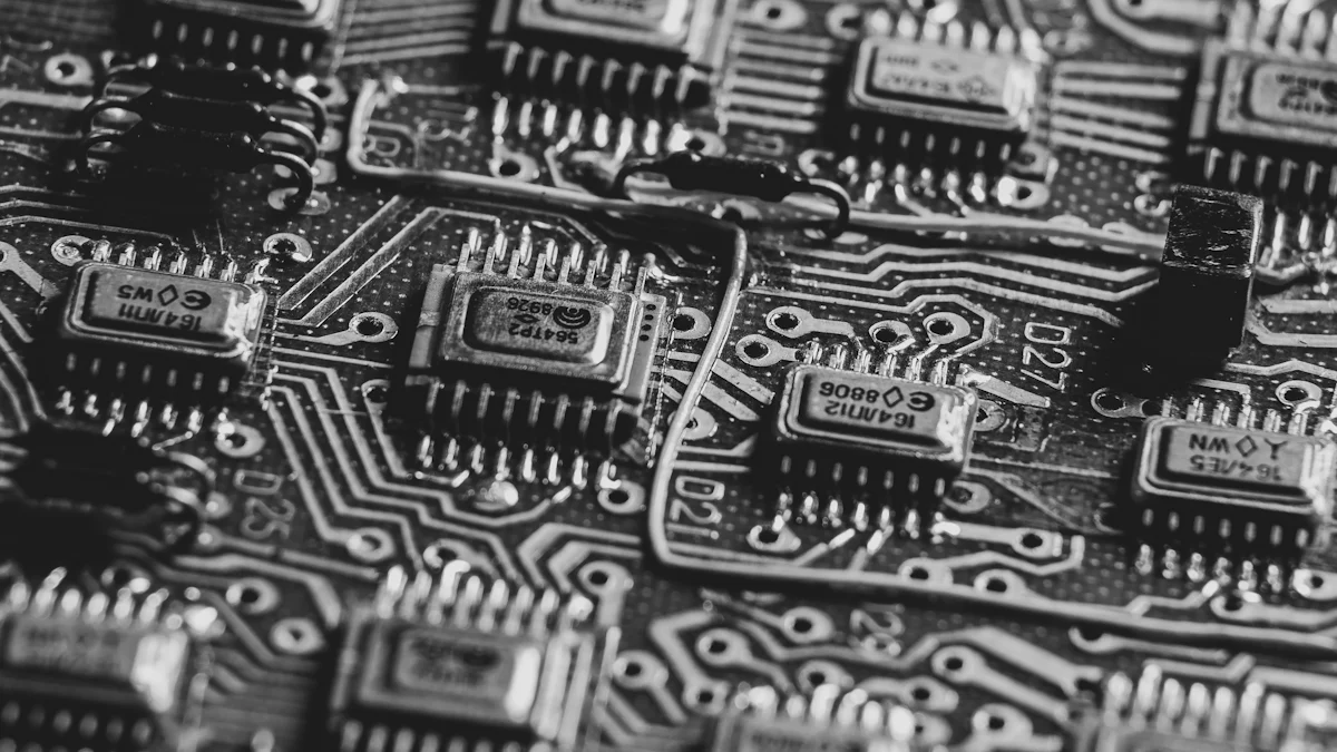
A Ball Grid Array (BGA) represents a modern surface-mount packaging technology for integrated circuits. Unlike traditional packaging methods that use pins or leads, BGA employs an array of solder balls on the underside of the package. These solder balls serve as both electrical and mechanical connections between the integrated circuit and the printed circuit board (PCB). This design allows for a higher density of connections within a smaller area, making BGA a preferred choice for compact and high-performance electronic devices.
Purpose of Ball Grid Array in Electronics
The primary purpose of BGA technology lies in its ability to meet the demands of modern electronics. As devices become smaller and more powerful, the need for efficient packaging solutions grows. BGA addresses this by offering:
Higher Input/Output (I/O) Density: The grid layout of solder balls enables more connections in a limited space, supporting high pin-count devices like microprocessors and GPUs.
Improved Electrical Performance: Shorter electrical paths reduce resistance and inductance, enhancing signal integrity and speed.
Enhanced Thermal Management: The design facilitates better heat dissipation, ensuring reliable performance in high-power applications.
These features make BGA indispensable in industries such as consumer electronics, automotive systems, and telecommunications.
Key Features of Ball Grid Array Technology
BGA technology stands out due to its unique characteristics, which include:
Compact Design: The use of solder balls on the entire underside of the package minimizes the footprint, making it ideal for space-constrained applications.
Low Profile: BGA packages have a slim form factor, which contributes to the sleek designs of modern electronic devices.
Durability and Reliability: The solder balls provide robust mechanical connections, reducing the risk of damage during assembly or operation.
Scalability: BGA supports high pin counts, making it suitable for advanced applications like ASICs, FPGAs, and memory chips.
Ease of Assembly: Automated processes can efficiently mount BGA components, lowering assembly failure rates and improving production efficiency.
"BGA technology replaces traditional leads with solder balls, offering more connections in a smaller area while improving thermal and electrical performance."
These features collectively position BGA as a cornerstone of modern electronic packaging, enabling the development of high-performance, compact, and reliable devices.
Advantages of Ball Grid Array Technology
Improved Electrical and Thermal Performance
Ball grid array technology significantly enhances electrical and thermal performance in electronic devices. The shorter electrical paths within BGA packages reduce inductance and capacitance, which improves signal integrity and supports higher-speed electrical performance. This feature makes BGA an ideal choice for high-frequency and high-speed applications, such as microprocessors and advanced communication systems.
The solder balls in BGA packages also provide excellent thermal conductivity. This design allows heat to dissipate efficiently from the integrated circuit (IC) to the printed circuit board (PCB). Effective heat dissipation ensures stable operation, even in high-power applications, and minimizes the risk of overheating. These attributes make BGA a preferred solution for devices requiring reliable thermal management, such as high-performance computing systems and automotive electronics.
"BGA packages excel in both electrical and thermal performance, offering reduced electrical noise and superior heat dissipation compared to traditional packaging methods."
Compact and Space-Saving Design
The compact design of ball grid array technology addresses the growing demand for miniaturized electronic devices. By utilizing the entire underside of the package for solder balls, BGA achieves a smaller footprint compared to traditional packaging methods like quad flat packages (QFP). This efficient use of space allows manufacturers to design slimmer and more portable devices without compromising functionality.
Additionally, the low-profile nature of BGA packages contributes to the sleek and lightweight designs of modern electronics. Devices such as smartphones, tablets, and wearable technology benefit from this space-saving feature, enabling advanced functionality in a compact form factor. The ability to integrate high-performance components into smaller spaces underscores the versatility of BGA technology in meeting the needs of contemporary electronics.
High-Density Connections for Enhanced Scalability
Ball grid array technology supports high-density connections, making it highly scalable for complex electronic assemblies. The grid layout of solder balls enables a higher pin count within a limited area, which is essential for devices requiring numerous input/output (I/O) connections. This feature is particularly advantageous for advanced applications like application-specific integrated circuits (ASICs), field-programmable gate arrays (FPGAs), and memory chips.
The scalability of BGA packages ensures compatibility with evolving technological demands. As electronic devices become more sophisticated, the need for packaging solutions that can accommodate increased functionality grows. BGA technology meets this demand by providing a reliable and efficient method for connecting high-performance components. Its ability to support high pin density while maintaining compactness positions BGA as a cornerstone of modern electronic design.
"The high-density connections offered by BGA technology enable scalability, making it a vital component in the development of advanced electronic systems."
Better Signal Integrity in High-Speed Applications
Ball grid array technology enhances signal integrity, making it a preferred choice for high-speed electronic applications. The shorter electrical paths within BGA packages minimize inductance and capacitance. This reduction ensures that signals experience less distortion and interference, which is critical for maintaining data accuracy in high-frequency operations. Devices like microprocessors and advanced communication systems benefit significantly from this feature.
The construction of BGA packages eliminates the long leads found in traditional packaging methods, such as quad flat packages (QFP). This design choice reduces electrical noise and improves overall performance. High-speed applications, including those in telecommunications and computing, demand such precision to handle rapid data transmission without compromising reliability.
"BGA packaging may be more suitable than QFN packaging in high-speed or high-frequency applications due to reduced electrical noise and signal integrity issues."
Moreover, the robust design of BGA packages ensures consistent performance even under demanding conditions. The solder balls provide stable connections, which further contribute to maintaining signal clarity. This reliability makes BGA an essential component in industries where high-speed data processing and transmission are paramount.
Disadvantages of Ball Grid Array Technology
Difficulty in Repair and Rework
Repairing and reworking ball grid array packages present significant challenges due to their unique design. The solder balls, located beneath the package, are not easily accessible. This hidden placement complicates the process of identifying and addressing defects. Technicians often require specialized equipment, such as X-ray inspection systems, to detect issues like solder joint failures. These tools increase the complexity and cost of repair operations.
Additionally, the rework process demands precision and expertise. Excessive heat during rework can damage the package or the printed circuit board (PCB). The risk of introducing new defects during rework further complicates the process. Compared to other packaging methods, such as quad flat packages (QFP), BGA packages require more advanced techniques and tools for successful repair and rework.
"The concealed solder joints in BGA packages make repair and rework more challenging, requiring advanced equipment and skilled technicians."
Higher Manufacturing and Assembly Costs
The manufacturing and assembly of ball grid array packages involve higher costs compared to conventional packaging methods. The intricate design of BGA packages necessitates advanced production techniques and specialized machinery. For instance, precise placement of solder balls and accurate alignment with the PCB demand automated assembly processes. These requirements increase the overall production expenses.
Moreover, the need for high-quality materials and stringent quality control measures adds to the cost. Manufacturers must ensure that solder balls meet specific standards to maintain electrical and mechanical reliability. In contrast, simpler packaging methods, such as QFP or quad flat no-lead (QFN), often incur lower production costs due to less complex designs and processes.
"BGA technology's advanced design and manufacturing requirements result in higher costs compared to traditional packaging methods."
Challenges in Inspecting Solder Joints
Inspecting solder joints in ball grid array packages poses significant difficulties. The solder balls are located underneath the package, making visual inspection impossible. Traditional inspection methods, such as optical microscopy, cannot assess the quality of these hidden connections. Manufacturers rely on advanced techniques, including X-ray imaging and automated optical inspection (AOI), to evaluate solder joint integrity.
These inspection methods, while effective, require substantial investment in equipment and training. The reliance on non-destructive testing techniques also increases the time and cost associated with quality assurance. In comparison, packaging methods like QFP allow for easier visual inspection of solder joints, reducing the need for specialized tools.
"The concealed nature of BGA solder joints necessitates advanced inspection methods, increasing both complexity and cost."
Potential Reliability Issues Under Mechanical Stress
Ball grid array packages face reliability challenges when subjected to mechanical stress. The solder balls, which serve as the primary connection points between the package and the printed circuit board (PCB), lack flexibility. This rigidity makes them more susceptible to damage under conditions such as vibration, bending, or thermal expansion. Devices operating in environments with frequent mechanical shocks or temperature fluctuations may experience solder joint failures, compromising their functionality.
Mechanical stress can cause cracks or fractures in the solder joints. These issues often arise due to the mismatch in the coefficient of thermal expansion (CTE) between the BGA package and the PCB. When exposed to repeated heating and cooling cycles, the materials expand and contract at different rates, leading to stress accumulation. Over time, this stress weakens the solder joints, increasing the likelihood of failure.
"The lack of compliance in BGA solder balls under mechanical stress can lead to reliability concerns, especially in demanding environments."
Compared to other packaging methods, such as quad flat no-lead (QFN) or quad flat packages (QFP), BGA packages exhibit higher sensitivity to mechanical stress. QFP packages, for instance, use leads that provide some degree of flexibility, reducing the impact of stress. However, BGA packages offer superior electrical performance and higher pin density, making them indispensable for high-speed and high-frequency applications despite these challenges.
To mitigate reliability issues, manufacturers often employ advanced materials and design techniques. Reinforced solder balls or underfill materials can enhance the mechanical strength of BGA packages. Additionally, proper PCB design, including the use of thermal relief pads and optimized trace layouts, can minimize stress concentration points. These measures ensure that BGA technology remains a viable solution for applications requiring high performance and compact designs.
When to Use Ball Grid Array Technology
Applications in Consumer Electronics
Ball grid array technology plays a pivotal role in consumer electronics, where compactness and performance are essential. Devices like smartphones, tablets, and gaming consoles rely on BGA packages to achieve high functionality within limited space. The ability of BGA to support high pin counts ensures seamless integration of advanced processors, memory chips, and other critical components. This packaging method also enhances thermal management, which is vital for maintaining the reliability of devices that operate continuously or under heavy loads.
Manufacturers in the consumer electronics industry benefit from the scalability of BGA. As demand for smaller and more powerful devices grows, BGA provides a solution that meets these requirements without compromising performance. Its low-profile design contributes to the sleek aesthetics of modern gadgets, making it a preferred choice for innovative product designs.
"BGA technology enables the development of compact, high-performance consumer electronics, meeting the demands of modern users."
Use in High-Performance Computing Systems
High-performance computing systems, such as servers, data centers, and advanced workstations, demand robust and efficient packaging solutions. Ball grid array technology addresses these needs by offering superior electrical performance and high-density connections. The shorter electrical paths in BGA packages reduce signal distortion, ensuring reliable data transmission in systems that process vast amounts of information at high speeds.
Thermal management is another critical factor in high-performance computing. BGA packages excel in dissipating heat, which helps maintain the stability and longevity of components operating under intense workloads. This capability makes BGA an indispensable choice for applications requiring consistent performance and reliability.
The scalability of BGA also supports the integration of cutting-edge technologies, such as artificial intelligence (AI) processors and machine learning algorithms. These systems rely on high-speed data processing, which BGA facilitates through its advanced design.
"BGA technology ensures optimal performance in high-computing environments by providing reliable connections and effective heat dissipation."
Ideal for Miniaturized and Portable Devices
Miniaturized and portable devices, such as wearable technology, medical implants, and IoT devices, benefit significantly from ball grid array technology. The compact design of BGA packages allows manufacturers to incorporate advanced functionalities into small form factors. This feature is crucial for devices where space constraints are a primary concern.
The durability of BGA packages ensures reliable performance in portable devices subjected to frequent movement and varying environmental conditions. The robust solder ball connections withstand mechanical stress, making BGA suitable for applications requiring mobility and resilience.
Moreover, the low-profile nature of BGA contributes to the lightweight design of portable devices. This characteristic enhances user comfort and convenience, particularly in wearable technology. The ability to combine compactness, durability, and high performance positions BGA as a key enabler of innovation in miniaturized electronics.
"BGA technology empowers the creation of portable and miniaturized devices, combining compactness with advanced functionality."
Scenarios Where Ball Grid Array Outperforms Other Packaging Methods
Ball grid array technology excels in specific scenarios where traditional packaging methods fall short. Its unique design and advanced features make it the preferred choice for applications requiring high performance, compactness, and reliability. Below are key scenarios where BGA outshines other packaging methods:
High-Density Applications
Devices with high pin-count requirements benefit significantly from BGA technology. The grid layout of solder balls allows for a higher number of connections within a smaller footprint. This feature makes BGA ideal for microprocessors, GPUs, and other components that demand numerous input/output (I/O) connections. In contrast, traditional methods like quad flat packages (QFP) struggle to achieve the same density without increasing the package size.Compact and Portable Devices
BGA packages enable the miniaturization of electronic devices. Their compact design and low profile make them suitable for smartphones, tablets, and wearable technology. These devices require advanced functionality in limited spaces, which BGA delivers efficiently. Traditional packaging methods often result in bulkier designs, limiting their use in space-constrained applications.High-Speed and High-Frequency Operations
BGA technology enhances signal integrity by reducing inductance and capacitance through shorter electrical paths. This feature ensures minimal signal distortion, making BGA the preferred choice for high-speed and high-frequency applications like advanced communication systems and high-performance computing. QFP and other methods, with their longer leads, often introduce electrical noise, compromising performance in such scenarios.Thermally Demanding Environments
Effective heat dissipation is critical in high-power applications. BGA packages excel in thermal management by facilitating efficient heat transfer from the integrated circuit (IC) to the printed circuit board (PCB). This capability ensures stable operation in thermally demanding environments, such as automotive electronics and data centers. Traditional packaging methods often lack the thermal efficiency required for these applications.Advanced Manufacturing Processes
Automated assembly processes benefit from the design of BGA packages. The uniform distribution of solder balls simplifies placement and reduces assembly failure rates. While QFP and similar methods require precise alignment of leads, BGA's design minimizes such challenges, improving production efficiency.
"BGA technology provides unmatched advantages in high-density, high-speed, and thermally demanding applications, making it indispensable in modern electronics."
Despite its advantages, BGA does require specialized inspection techniques, such as X-ray imaging, to ensure solder joint quality. This necessity arises because the solder balls are concealed beneath the package, making visual inspection impossible. However, the benefits of BGA in terms of performance and scalability outweigh these challenges in most scenarios.
Ball grid array technology has become a cornerstone in modern electronics, offering unmatched performance, compactness, and scalability. Its ability to support high-density connections and efficient thermal management makes it indispensable for advanced applications. Engineers must carefully evaluate specific requirements, such as mechanical reliability and inspection challenges, to maximize its potential. By leveraging its strengths and addressing its limitations with innovative techniques, BGA technology continues to drive progress in consumer electronics, high-performance computing, and miniaturized devices.
See Also
Innovations Shaping Huizhou Zhongkai High-tech Zone's Future
Transforming Semiconductor Displays: Zhongkai's Major Investment Initiative
Smart Device Manufacturing Hub: Easily Reach EVE Energy
Zhongkai High-tech Zone: Center for Smart Device Advancements

Zhongkai High tech Zone National foreign trade transformation and Upgradi Base(Electronic Information)Cloud Platform.
Address: Zhongkai High-tech Zone,Huizhou City ,Guangdong,China
E-mail: huizhoueii@163.com 13510001271@163.com
Tel: +86-0752-3279220 Mobile: +86-13510001271