Printed Circuit Boards: Definition and Operation

A printed circuit board serves as the foundation of modern electronics, enabling seamless integration of components into a unified system. Its flat, layered design supports electronic parts while facilitating electrical connections through conductive pathways. Copper layers within the board act as primary channels for electrical signals, ensuring efficient performance. PCBs power essential devices like smartphones, computers, and appliances, driving innovation in consumer technology. The global PCB market reflects its significance, with projections estimating growth from $84 billion in 2023 to $168.5 billion by 2036. This growth underscores the indispensable role of PCBs in advancing technology.
Key Takeaways
Printed circuit boards (PCBs) are essential for modern electronics, providing the foundation for devices like smartphones and computers.
Understanding the layered structure of PCBs—substrate, conductive, solder mask, and silkscreen—is crucial for grasping their functionality.
Different types of PCBs, including single-layer, double-layer, and multilayer, cater to various applications, from simple household gadgets to complex medical equipment.
Flexible and rigid-flex PCBs offer unique advantages, such as adaptability and durability, making them ideal for compact and high-performance devices.
The manufacturing process of PCBs involves careful design, prototyping, etching, and component assembly to ensure reliability and performance.
Incorporating both passive and active components on PCBs enhances their versatility, enabling a wide range of functionalities in electronic devices.
As the PCB market is projected to grow significantly, understanding their role can empower individuals and businesses to innovate in technology.
The Structure of a Printed Circuit Board
Printed circuit boards consist of multiple layers, each serving a specific purpose. These layers work together to provide mechanical support and enable the flow of electrical signals. Understanding these layers is essential for grasping how PCBs function.
Layers of a Printed Circuit Board
Substrate layer: The base material providing mechanical support.
The substrate layer forms the foundation of a printed circuit board. Typically made from fiberglass-reinforced epoxy resin or other insulating materials, it provides the necessary rigidity and durability. This layer ensures that the PCB can withstand physical stress and environmental factors while maintaining its structural integrity.
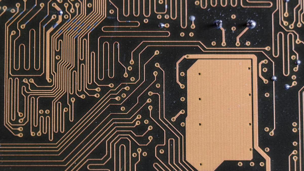
Conductive layer: Copper traces that carry electrical signals.
The conductive layer consists of thin sheets of copper laminated onto the substrate. These copper traces act as pathways for electrical signals, connecting various components on the board. Engineers carefully design these traces to optimize signal flow and minimize interference, ensuring reliable performance.
Solder mask layer: A protective layer that prevents short circuits.
The solder mask layer covers the copper traces, protecting them from oxidation and accidental contact. This layer also prevents solder bridges during the assembly process, reducing the risk of short circuits. Its distinct green color is a common visual characteristic of most PCBs.
Silkscreen layer: Printed labels and markings for component placement.
The silkscreen layer contains printed symbols, text, and markings that guide the placement of components. It helps manufacturers and technicians identify parts, test points, and connection points. This layer enhances the usability and accuracy of the PCB during assembly and maintenance.
How Layers Work Together in a Printed Circuit Board
The layers of a printed circuit board operate in harmony to ensure functionality. The substrate provides a stable base, while the conductive layer facilitates electrical connections. The solder mask protects these connections, and the silkscreen offers clarity for assembly. Together, these layers create a compact and efficient system that supports modern electronic devices.
Types of Printed Circuit Boards and Their Applications
Printed circuit boards come in various types, each tailored to specific applications and design requirements. The choice of PCB type depends on factors like circuit complexity, device functionality, and manufacturing considerations.
Single-layer Printed Circuit Boards
Single-layer PCBs, also known as single-sided PCBs, feature a single conductive layer of copper on one side of the substrate. These boards are simple in design and cost-effective to produce. They are ideal for straightforward electronic devices that do not require complex circuitry.
Applications: Single-layer PCBs are commonly used in household appliances, calculators, and LED lighting systems. Their simplicity makes them suitable for devices with minimal power and signal requirements.
Double-layer Printed Circuit Boards
Double-layer PCBs, or double-sided PCBs, have conductive copper layers on both sides of the substrate. This design doubles the available area for circuit traces, enabling more complex connections. Engineers use vias, or small holes, to connect the two layers, allowing signals to pass between them.
Applications: Double-layer PCBs are widely used in automotive dashboards, industrial controls, and audio equipment. Their ability to handle greater circuit density makes them suitable for devices requiring moderate complexity.
Multilayer Printed Circuit Boards
Multilayer PCBs consist of three or more conductive layers, separated by insulating materials. These layers are stacked and laminated together, creating a compact structure capable of supporting intricate circuits. Multilayer PCBs excel in signal integrity and power distribution, making them indispensable for advanced electronics.
Applications: Multilayer PCBs are essential in high-performance devices like computers, servers, and medical equipment. They are also used in graphics cards, motherboards, and other hardware requiring dense and complex circuitry.
Specialized Printed Circuit Boards (Flexible and Rigid-Flex)
Specialized printed circuit boards, such as flexible and rigid-flex PCBs, cater to unique design and application needs. These boards offer enhanced adaptability and durability, making them indispensable in advanced electronics.
Flexible Printed Circuit Boards
Flexible PCBs, often referred to as flex circuits, use a flexible substrate material like polyimide. This flexibility allows the board to bend, twist, or fold without damaging the circuitry. Engineers design these boards for applications where space constraints or dynamic movements are critical.
Advantages:
Lightweight and compact design.
Resistance to vibrations and mechanical stress.
Ability to fit into irregularly shaped devices.
Applications: Flexible PCBs are widely used in wearable devices, medical implants, and aerospace systems. Their adaptability makes them ideal for products requiring compact and lightweight solutions.
Rigid-Flex Printed Circuit Boards
Rigid-flex PCBs combine the benefits of both rigid and flexible boards. They consist of multiple layers of flexible circuits attached to rigid sections. This hybrid design provides the structural support of rigid boards while retaining the flexibility of flex circuits.
Advantages:
Enhanced reliability due to fewer connectors and solder joints.
Improved signal integrity in complex designs.
Space-saving design for compact devices.
Applications: Rigid-flex PCBs are commonly found in smartphones, cameras, and military equipment. Their ability to integrate multiple functionalities within a single board makes them suitable for high-performance devices.
Both flexible and rigid-flex PCBs demonstrate the versatility of printed circuit board technology. By addressing specific challenges in modern electronics, these specialized boards enable innovative designs and applications.
Common Components Found on a Printed Circuit Board
Printed circuit boards rely on various components to perform their intended functions. These components fall into distinct categories based on their roles in the circuit. Each type contributes to the overall operation and efficiency of the board.
Passive Components
Passive components do not generate energy but influence electrical signals in specific ways. They play a crucial role in regulating and stabilizing circuits.
Resistors: Control current flow.
Resistors limit the flow of electrical current within a circuit. Engineers use them to manage voltage levels and protect sensitive components from excessive current. Resistors come in various sizes and resistance values, allowing precise control over circuit behavior. Their placement on a printed circuit board ensures that electrical signals remain within safe operating limits.
Capacitors: Store and release electrical energy.
Capacitors temporarily store electrical energy and release it when needed. This ability helps stabilize voltage levels and filter out noise in a circuit. Capacitors are essential for maintaining consistent power delivery to components. Their design includes two conductive plates separated by an insulating material, enabling efficient energy storage and discharge.
Active Components
Active components generate or amplify electrical signals. They are vital for enabling complex functionalities in electronic devices.
Transistors: Amplify or switch electrical signals.
Transistors serve as the building blocks of modern electronics. They amplify weak electrical signals, making them stronger and more usable. Additionally, transistors act as switches, controlling the flow of current in a circuit. Their small size and versatility make them indispensable in applications ranging from microprocessors to power management systems.
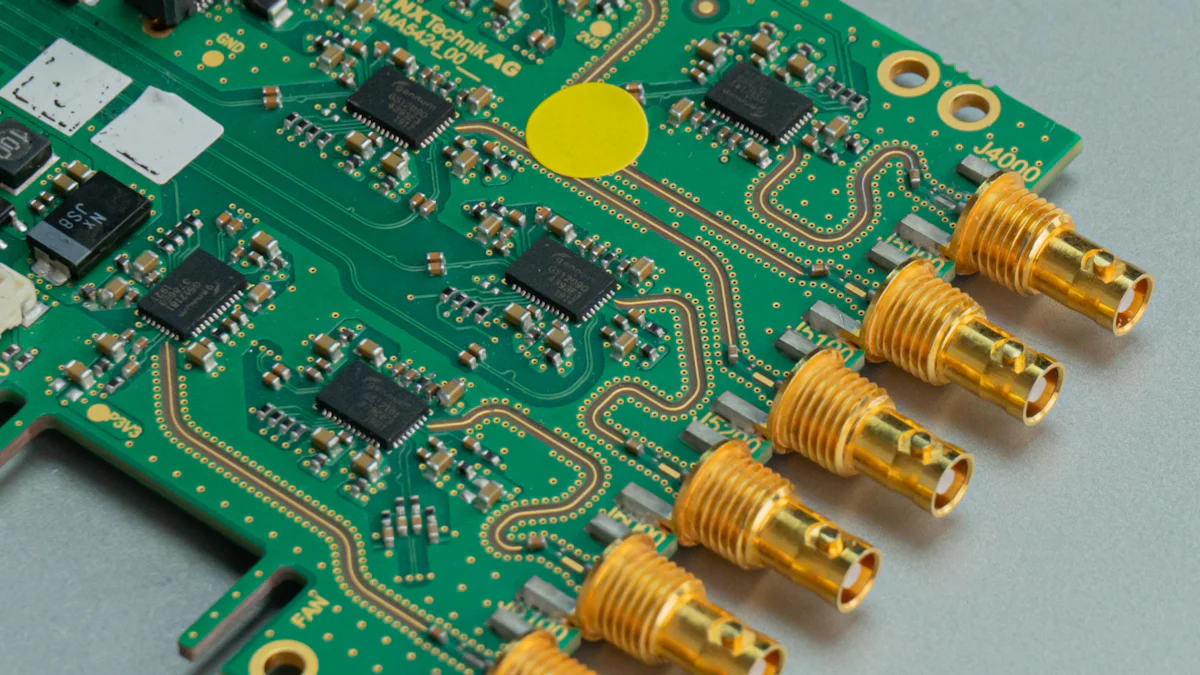
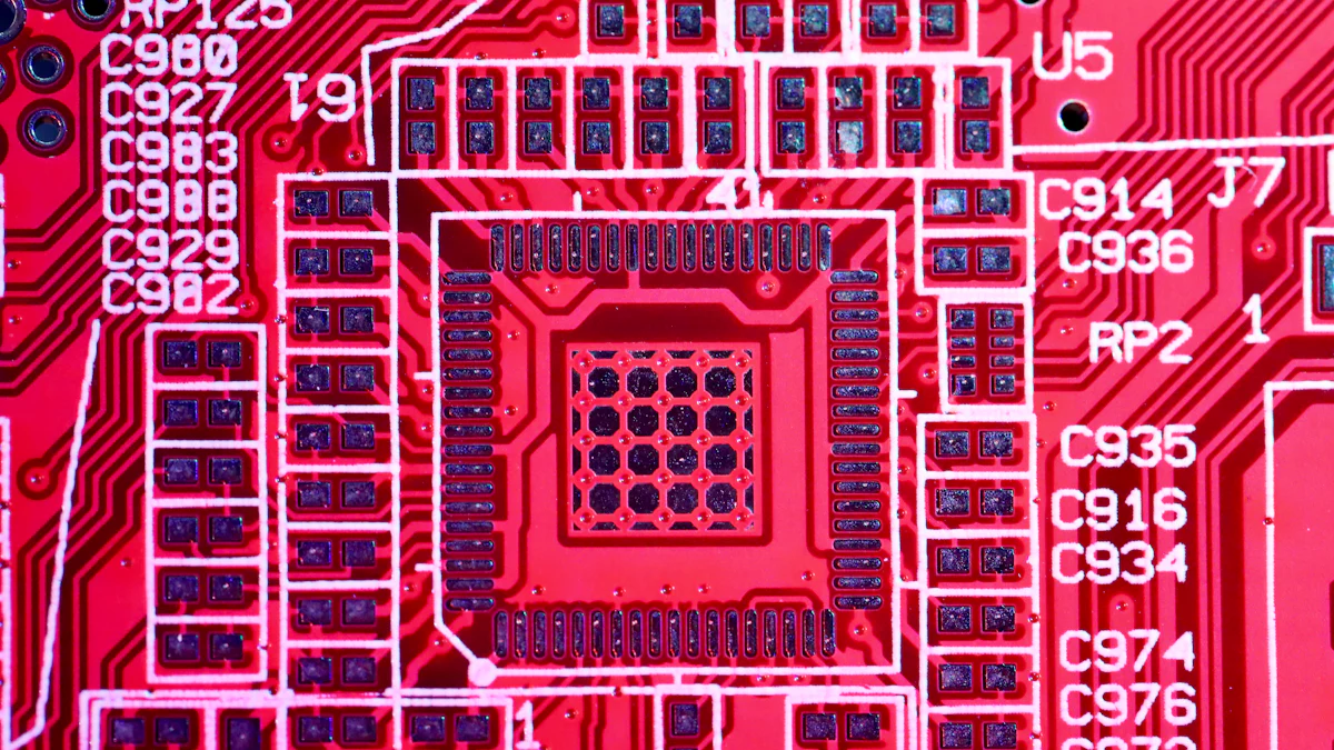
Integrated Circuits (ICs): Perform complex functions.
Integrated circuits, or ICs, combine multiple electronic components into a single chip. These chips perform complex tasks such as data processing, signal amplification, and memory storage. ICs reduce the size and complexity of circuits while enhancing performance. Their integration into printed circuit boards enables advanced functionalities in compact devices.
Connectors and Other Components
Connectors establish physical and electrical connections between the printed circuit board and external devices. They facilitate communication and power transfer, ensuring seamless integration with other systems. Additional components, such as diodes and inductors, further enhance the board's capabilities by providing specialized functions like signal rectification and energy storage.
Expert Testimony:
"The latest innovation in PCB technology—the rigid flex PCB—combines the complexity and reliability of a hardboard circuit with flexible layers that are incorporated into the rigid structure. With these combined layers, rigid-flex PCBs are smaller, thinner and can fit into unusually shaped or especially small products."
This statement highlights the importance of components like connectors and ICs in enabling compact and efficient designs, particularly in advanced PCB types.
By combining passive and active components with connectors, printed circuit boards achieve remarkable versatility. These elements work together to support the functionality of modern electronic devices, from simple household gadgets to sophisticated industrial systems.
How a Printed Circuit Board Works
Printed circuit boards operate by facilitating the flow of electrical signals between components. Their design ensures that each component performs its specific function while maintaining the integrity of the overall circuit. The interaction between components and the pathways on the board determines the functionality of the device.
Electrical Signal Flow in a Printed Circuit Board
Electrical signal flow begins when power is supplied to the printed circuit board. The conductive copper traces act as highways, directing electrical signals to various components. These signals enable components like resistors, capacitors, and transistors to perform their roles. Resistors control current flow, ensuring that sensitive components receive the correct amount of energy. Capacitors store and release electrical energy, stabilizing voltage levels and filtering out noise. Transistors amplify or switch signals, enabling complex operations within the circuit.
Example: Decoupling capacitors, often placed near the power pins of integrated circuits (ICs), filter out noise and ensure a stable power supply. This stability is crucial for maintaining consistent performance in electronic devices.
The flow of signals also involves active components like diodes and ICs. Diodes allow current to flow in one direction, protecting the circuit from potential damage. ICs integrate multiple functions into a single chip, reducing the complexity of the circuit while enhancing its capabilities. Connectors play a vital role by linking the PCB to external devices, enabling communication and power transfer.
The Role of Design in Printed Circuit Board Operation
The design of a printed circuit board directly impacts its operation. Engineers carefully plan the layout to optimize signal flow and minimize interference. The placement of components, the width of copper traces, and the use of vias all contribute to the board's efficiency. For instance, multilayer PCBs allow for more complex designs by stacking multiple conductive layers, improving signal integrity and power distribution.
Expert Insight: "The integration of flexible and rigid-flex PCBs has revolutionized design possibilities. These boards combine adaptability with structural support, making them ideal for compact and high-performance devices."
Design considerations also include the selection of materials. The substrate layer provides mechanical support, while the solder mask protects copper traces from oxidation. The silkscreen layer adds clarity by marking component placement, aiding in assembly and maintenance. Engineers must balance these elements to create a reliable and efficient PCB.
In advanced applications, specialized PCBs like flexible and rigid-flex boards address unique challenges. Flexible PCBs bend and twist to fit into irregularly shaped devices, while rigid-flex boards combine flexibility with durability. These innovations demonstrate how design influences the functionality and versatility of printed circuit boards.
Overview of the Printed Circuit Board Manufacturing Process
The manufacturing process of a printed circuit board involves several precise steps. Each stage ensures the board's functionality, durability, and reliability. From initial design to final assembly, every phase contributes to creating a high-quality PCB.
Design and Prototyping
The process begins with designing the PCB layout. Engineers use specialized software to map out the placement of components and the routing of electrical pathways. This step ensures optimal signal flow and minimizes interference. Proper design is critical for maintaining signal integrity, especially in high-speed PCBs where even minor distortions can lead to data corruption or system failure.
Prototyping follows the design phase. Manufacturers create a small batch of PCBs to test the design's functionality and identify potential issues. This step allows engineers to refine the layout and ensure the board meets performance requirements. Prototyping reduces the risk of errors in mass production, saving time and resources.
Key Insight: "Flex PCB layout design considerations are crucial for ensuring the reliability and durability of the PCB. Proper layout design and routing can prevent stress points and damage to copper circuits."
Etching and Layering
Once the design is finalized, the manufacturing process moves to etching and layering. A thin layer of copper is laminated onto the substrate material. Using a chemical etching process, manufacturers remove excess copper, leaving behind the desired circuit patterns. This step forms the conductive pathways that connect the components.
For multilayer PCBs, additional layers are added during this phase. Insulating materials separate each conductive layer, ensuring electrical isolation. The layers are then aligned and bonded together through a lamination process. This creates a compact structure capable of supporting complex circuits.
Fact: Advancements in materials and manufacturing processes have significantly improved PCB capabilities. These innovations enhance performance and boost reliability in electronic devices.
Component Assembly and Soldering
The final stage involves assembling components onto the PCB. Automated machines place components like resistors, capacitors, and integrated circuits onto the board. Precision is essential to ensure proper alignment and functionality.
Soldering secures the components to the board. During this process, solder paste is applied to the contact points, and the board passes through a reflow oven. The heat melts the solder, creating strong electrical connections. For double-sided or multilayer PCBs, through-hole components may require additional soldering techniques.
After assembly, manufacturers conduct rigorous testing to verify the PCB's performance. Quality control ensures that the board meets industry standards and functions as intended.
Expert Note: "PCBs optimize electrical pathways, enhance performance, and boost reliability in electronic devices. Proper assembly and soldering are vital for achieving these benefits."
Printed circuit boards have revolutionized the electronics industry since their inception in the 1930s, laying the groundwork for modern technological advancements. Their compact design and efficient functionality make them indispensable in countless devices. By understanding their structure, types, and components, one can appreciate their pivotal role in enabling innovation. As industries evolve, PCBs will continue to adapt, driving progress in fields like healthcare, aerospace, and consumer electronics. Their significance underscores the ongoing pursuit of smarter, more efficient solutions in technology.
See Also
Transforming Semiconductor Displays: Zhongkai's Billion-Dollar Investment Initiative
Boosting Electronic Information: The Progress of Zhongkai High-tech Zone
Zhongkai High-tech Zone: Leading the Charge in Electronic Innovation
Zhongkai High-tech Zone: Enhancing Global Edge in Electronics
Zhongkai High-tech Zone: A Booming Hub for Electronic Information

Zhongkai High tech Zone National foreign trade transformation and Upgradi Base(Electronic Information)Cloud Platform.
Address: Zhongkai High-tech Zone,Huizhou City ,Guangdong,China
E-mail: huizhoueii@163.com 13510001271@163.com
Tel: +86-0752-3279220 Mobile: +86-13510001271