The Surprising Role of Dual in-line Packages

The dual in-line package represents a pivotal innovation in electronic component packaging. Its design, featuring two parallel rows of pins, ensures efficient connectivity and straightforward assembly. Introduced in the mid-1960s, it quickly became a standard in the semiconductor industry due to its reliability and simplicity. Despite advancements in surface-mount technology, this packaging remains indispensable in specific areas. Prototyping, educational tools, and legacy systems continue to rely on its robust structure. Its enduring relevance highlights the balance between traditional designs and modern technological demands.
Key Takeaways
Dual in-line packages (DIPs) are essential for prototyping and educational purposes due to their user-friendly design and ease of assembly.
DIPs provide reliable protection for integrated circuits, making them ideal for legacy systems and vintage electronics that require maintenance.
The cost-effectiveness of DIPs allows hobbyists and small businesses to utilize them without the need for expensive equipment, promoting innovation.
DIPs excel in environments where durability and reliability are critical, ensuring consistent performance even in demanding conditions.
Despite the rise of surface-mount technology (SMT), DIPs remain relevant in specific applications, bridging traditional designs with modern technology.
Educational institutions benefit from using DIPs to teach fundamental electronics concepts, providing students with hands-on experience in circuit assembly.
While DIPs face challenges in size and compatibility with modern technologies, their simplicity and robustness ensure their continued use in niche applications.
What Are Dual in-line Packages?

Design and Structure
The dual in-line package (DIP) features a rectangular housing with two parallel rows of metallic pins extending from opposite sides. These pins serve as electrical connectors, enabling seamless integration with printed circuit boards (PCBs). Manufacturers typically construct the housing from ceramic or plastic materials, ensuring durability and reliability. The standardized dimensions of DIPs comply with JEDEC standards, which simplifies their compatibility with various electronic systems.
This design promotes ease of handling and installation. The through-hole configuration allows users to insert the pins into pre-drilled holes on PCBs, followed by soldering for a secure connection. This straightforward assembly process makes DIPs particularly suitable for prototyping and educational purposes. Additionally, the layout of the pins facilitates efficient airflow around the component, aiding in heat dissipation and improving thermal management.
DIPs come in various pin counts, ranging from 8 to 64 or more, depending on the complexity of the integrated circuit housed within. This versatility enables their use in a wide range of applications, from simple logic gates to advanced microcontrollers and memory chips. The robust structure of DIPs ensures their longevity, even in demanding environments.
Purpose and Functionality
The primary purpose of the dual in-line package is to house and protect integrated circuits (ICs) while providing a reliable interface for electrical connections. By encapsulating ICs within a sturdy casing, DIPs shield sensitive components from environmental factors such as dust, moisture, and physical damage. This protective feature enhances the overall reliability of electronic devices.
DIPs play a critical role in connecting ICs to PCBs. The parallel rows of pins establish electrical pathways between the internal circuitry of the IC and the external components of the electronic system. This connectivity enables the seamless operation of devices, ensuring that signals and power flow efficiently throughout the circuit.
In addition to their protective and connective functions, DIPs support a wide array of applications. They are commonly used in logic gates, operational amplifiers, timer ICs, microcontrollers, and memory chips. Their versatility extends to consumer electronics, industrial equipment, and automotive systems. The simplicity and reliability of DIPs make them a cornerstone of integrated circuit packaging, even as newer technologies emerge.
The Role of Dual in-line Packages in Modern Electronics
Applications in Legacy Systems
The dual in-line package continues to play a vital role in legacy systems. Many older electronic devices, designed before the widespread adoption of surface-mount technology, rely on DIP components for functionality. These systems often include vintage computers, industrial machinery, and early consumer electronics. The standardized design of DIPs ensures compatibility with these older technologies, making them indispensable for maintenance and repair.
Legacy systems benefit from the durability and reliability of DIP components. Their robust structure withstands environmental stress, ensuring consistent performance over time. Technicians and engineers frequently use DIPs to replace outdated or damaged parts in legacy equipment. This practice extends the lifespan of these systems, reducing the need for costly upgrades or replacements.
Moreover, the adaptability of DIPs allows them to bridge the gap between old and new technologies. Engineers often integrate DIP components into hybrid systems, combining traditional designs with modern innovations. This approach preserves the functionality of legacy systems while introducing enhanced capabilities.
Prototyping and Development
Prototyping and development processes heavily rely on the dual in-line package due to its user-friendly design. DIPs are ideal for breadboards and prototyping boards, where components must be easily inserted, removed, and rearranged. Their through-hole configuration simplifies manual handling, enabling engineers to test and refine circuit designs efficiently.
The versatility of DIPs supports a wide range of applications during development. Engineers use them to prototype logic circuits, microcontrollers, and memory modules. Their straightforward assembly process reduces the time and effort required to create functional prototypes. This efficiency accelerates the development cycle, allowing faster transitions from concept to production.
DIPs also excel in low-volume production scenarios. Their cost-effectiveness and ease of assembly make them suitable for small-scale manufacturing, where advanced packaging technologies may not be practical. This adaptability ensures that DIPs remain a valuable tool for innovators and hobbyists alike.
Educational Use
Educational institutions frequently incorporate the dual in-line package into their curricula. Its simple design and ease of use make it an excellent teaching tool for students learning about electronics. DIPs provide a hands-on experience, allowing learners to assemble and test circuits without requiring specialized equipment.
Instructors often use DIPs to demonstrate fundamental concepts such as logic gates, amplifiers, and timers. These components offer a tangible way to explore the principles of circuit design and functionality. Students gain practical skills by working with DIPs, preparing them for careers in engineering and technology.
The affordability of DIPs further enhances their value in education. Schools and universities can acquire these components at a low cost, making them accessible to a wide range of learners. This accessibility fosters innovation and creativity, encouraging students to experiment and develop their own projects.
DIPs also serve as a bridge between theoretical knowledge and real-world applications. By working with these components, students gain insights into the challenges and opportunities of electronic design. This hands-on approach cultivates problem-solving skills and a deeper understanding of the field.
Advantages of Dual in-line Packages
Ease of Use
The dual in-line package simplifies the assembly and handling of electronic components. Its through-hole design allows users to insert pins into pre-drilled holes on printed circuit boards (PCBs) with minimal effort. This straightforward process makes it ideal for manual soldering, especially in prototyping and small-scale production. The accessibility of the pins ensures that engineers and technicians can easily connect or replace components without requiring advanced tools.
Educational institutions and hobbyists benefit significantly from this ease of use. Students learning electronics can quickly grasp the fundamentals of circuit assembly by working with DIPs. The design encourages hands-on experimentation, fostering a deeper understanding of electronic systems. Additionally, the layout of the pins reduces the likelihood of errors during assembly, enhancing the reliability of prototypes and educational projects.
Cost-Effectiveness
The dual in-line package offers a cost-effective solution for various electronic applications. Its manufacturing process involves relatively simple materials like plastic or ceramic, which keeps production costs low. This affordability makes DIPs accessible to a wide range of users, from large-scale manufacturers to individual hobbyists.
In comparison to surface-mount technology (SMT), DIPs require less specialized equipment for assembly. Manual soldering eliminates the need for expensive automated machinery, reducing initial investment costs for small businesses and educational institutions. Furthermore, the durability of DIPs minimizes the frequency of replacements, contributing to long-term cost savings.
DIPs also support multiple voltage and current ratings, making them versatile across different applications. Their ability to operate within a wide temperature range ensures consistent performance in various environments. This adaptability further enhances their value, particularly in scenarios where budget constraints demand reliable yet economical solutions.
Reliability
Reliability remains a hallmark of the dual in-line package. Its robust structure protects the internal circuitry from physical damage, dust, and moisture. This durability ensures consistent performance, even in demanding conditions. Engineers often choose DIPs for legacy systems and industrial applications where long-term reliability is critical.
The design of DIPs promotes efficient thermal management. The spacing between the pins allows for better airflow, which aids in heat dissipation. This feature reduces the risk of overheating, extending the lifespan of the components. Additionally, the secure soldering of pins to PCBs ensures stable electrical connections, minimizing the chances of circuit failure.
DIPs excel in applications requiring frequent testing and adjustments. Their ease of handling and reusability make them a preferred choice for prototyping and development. Unlike SMT components, which can be challenging to remove and replace, DIPs allow engineers to modify circuits with minimal disruption. This flexibility underscores their reliability in dynamic and evolving projects.
Limitations and Challenges of Dual in-line Packages
Size and Bulkiness
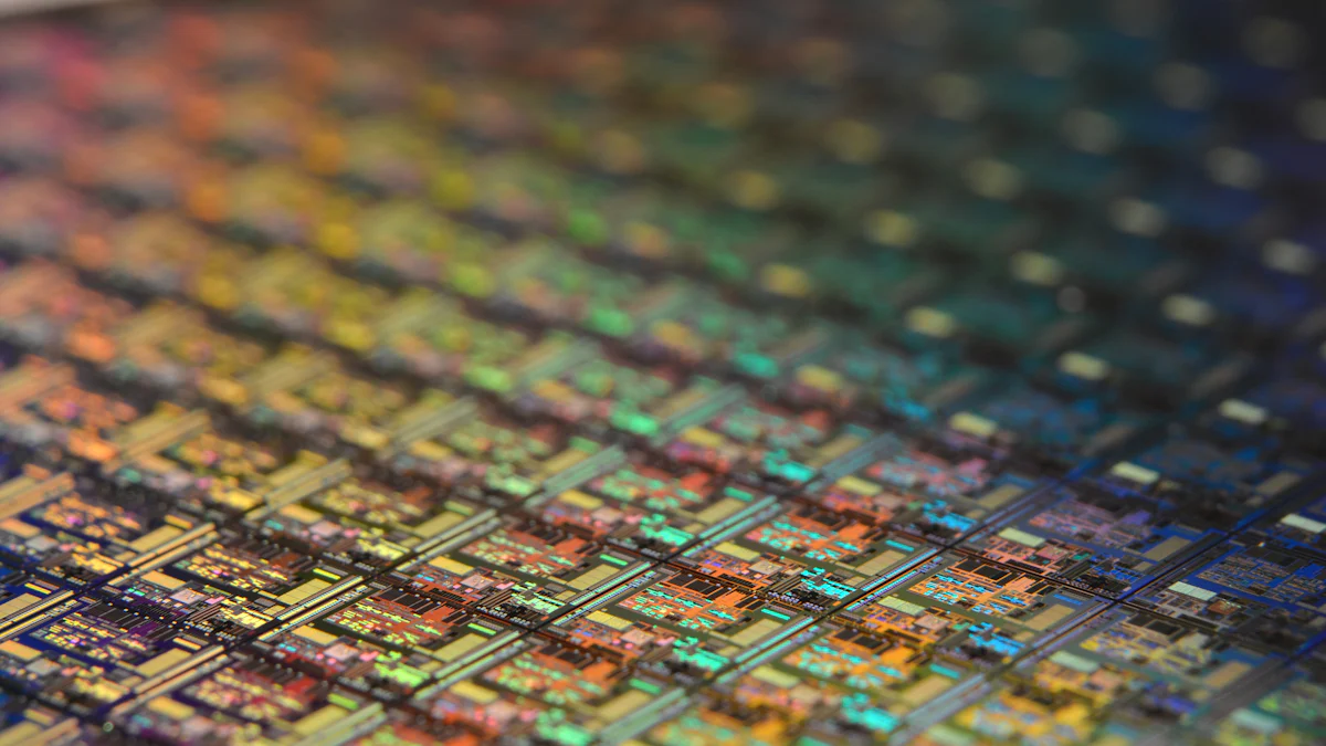
Dual in-line packages (DIPs) often face criticism for their size and bulkiness. Their through-hole design, while advantageous for prototyping and educational purposes, requires significant space on printed circuit boards (PCBs). This characteristic limits their suitability for compact and high-density electronic designs. Modern devices, such as smartphones and wearables, demand smaller components to accommodate advanced functionalities within minimal physical dimensions. DIPs struggle to meet these requirements due to their relatively large footprint.
The limited pin count of DIPs further exacerbates this issue. Most DIPs feature a restricted number of pins, typically ranging from 8 to 64. This limitation makes them unsuitable for complex integrated circuits (ICs) that require numerous connections. As a result, engineers often turn to alternative packaging technologies for applications involving high-density integration. The inability of DIPs to support intricate designs highlights their constraints in modern electronics.
"The increasing demand for smaller, more compact electronic devices has driven the shift away from DIPs toward advanced packaging solutions like surface-mount technology (SMT)."
Despite these challenges, DIPs remain relevant in specific contexts where size and pin count are less critical. Their robustness and ease of use continue to make them valuable for legacy systems and educational settings.
Compatibility with Modern Technologies
The compatibility of dual in-line packages with modern technologies presents another significant challenge. As the electronics industry evolves, new packaging methods, such as SMT, have emerged to address the limitations of traditional designs. SMT components offer smaller footprints, lower profiles, and enhanced thermal performance, making them ideal for contemporary applications. In contrast, DIPs often struggle to integrate seamlessly with advanced systems.
The through-hole configuration of DIPs requires manual soldering and pre-drilled holes on PCBs, which increases assembly time and costs. Modern manufacturing processes favor automated techniques that streamline production and reduce expenses. This shift has further marginalized the role of DIPs in large-scale manufacturing.
Additionally, the physical design of DIPs limits their compatibility with cutting-edge technologies. High-speed circuits and miniaturized devices demand packaging solutions that minimize signal interference and optimize performance. DIPs, with their larger size and pin spacing, cannot meet these stringent requirements. Engineers frequently opt for SMT or other advanced packaging methods to achieve superior results.
While DIPs face challenges in adapting to modern technologies, they continue to serve niche applications. Their simplicity and reliability ensure their enduring presence in prototyping, education, and legacy systems.
Dual in-line Packages vs. Other Packaging Technologies
Comparison with Surface-Mount Technology (SMT)
Dual in-line packages (DIPs) and surface-mount technology (SMT) represent two distinct approaches to electronic component packaging. Each offers unique advantages tailored to specific applications. DIPs excel in simplicity and reliability, making them ideal for prototyping, educational purposes, and legacy systems. Their through-hole design allows for easy manual soldering, which benefits engineers and hobbyists working on small-scale projects.
In contrast, SMT has revolutionized modern electronics with its compact design and advanced capabilities. SMT components feature smaller footprints and lower profiles, enabling high-density integration on printed circuit boards (PCBs). This packaging method supports automated assembly processes, reducing production time and costs for large-scale manufacturing. Additionally, SMT provides superior thermal performance, optimizing heat dissipation in high-speed circuits.
"The increasing demand for miniaturization in electronics has driven the shift from DIPs to SMT, particularly in consumer devices like smartphones and wearables."
Despite these advancements, DIPs maintain a foothold in areas where size and automation are less critical. Their robust structure and straightforward assembly process ensure continued relevance in specific contexts. SMT, however, dominates industries requiring compact designs and high-frequency performance.
Relevance in Modern Electronics
The role of dual in-line packages in modern electronics remains significant, despite the dominance of newer technologies like SMT. DIPs continue to serve as a cornerstone in prototyping and development. Their ease of use allows engineers to test and refine circuit designs without the need for specialized equipment. Educational institutions also rely on DIPs to teach fundamental concepts, providing students with hands-on experience in circuit assembly.
Legacy systems further highlight the importance of DIPs. Many older devices, including industrial machinery and vintage computers, depend on DIP components for maintenance and repair. The standardized design of DIPs ensures compatibility with these systems, extending their operational lifespan.
While SMT addresses the demands of high-density integration and miniaturization, DIPs offer unmatched versatility in specific applications. Their ability to bridge traditional and modern technologies underscores their enduring value. Engineers often integrate DIPs into hybrid systems, combining the reliability of older designs with the efficiency of contemporary innovations.
In summary, DIPs and SMT cater to different needs within the electronics industry. DIPs thrive in prototyping, education, and legacy systems, while SMT leads in compact, high-performance applications. Together, they illustrate the diverse requirements of modern electronics, ensuring that both technologies remain indispensable in their respective domains.
Dual in-line packages (DIPs) continue to hold a unique position in modern electronics. Their simplicity and robustness make them indispensable in legacy systems, prototyping, and educational environments. These components bridge the gap between traditional designs and contemporary needs, offering reliability and ease of use.
"Legacy systems and educational settings will keep DIPs alive for their simplicity and ease of handling."
As the electronics landscape evolves, DIPs will maintain their niche applications. Their enduring relevance highlights the balance between innovation and foundational technologies, ensuring their role in fostering creativity and preserving functionality.
See Also
Transforming Semiconductor Displays: Zhongkai's Major Investment Insights
Zhongkai's Breakthrough in High-Energy Battery Technology
Innovating for Tomorrow: Huizhou Zhongkai's Development Vision

Zhongkai High tech Zone National foreign trade transformation and Upgradi Base(Electronic Information)Cloud Platform.
Address: Zhongkai High-tech Zone,Huizhou City ,Guangdong,China
E-mail: huizhoueii@163.com 13510001271@163.com
Tel: +86-0752-3279220 Mobile: +86-13510001271