Effortless Tips for Using Dual In-line Packages

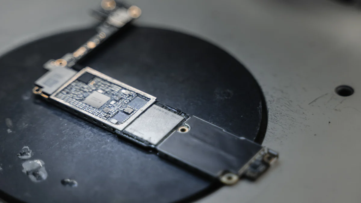
A Dual in-line package is a rectangular electronic component featuring two parallel rows of pins. This design simplifies the integration of integrated circuits (ICs) into printed circuit boards (PCBs). Its straightforward structure allows users to either solder it directly onto a PCB or insert it into a socket for easy replacement. The package is widely appreciated for its reliability, low cost, and compatibility with breadboards, making it an ideal choice for educational projects, prototyping, and small-scale electronics. Its versatility ensures accessibility for hobbyists and professionals alike, fostering innovation and experimentation in electronics.
Key Takeaways
Understand the physical structure of DIPs to ensure proper handling and installation, which enhances reliability in your projects.
Always refer to the datasheet for pin configurations and electrical characteristics to avoid errors during integration.
Use sockets for DIPs to simplify replacements and protect the component during testing and repairs.
Test your circuit on a breadboard before soldering to identify potential issues and optimize your design.
Maintain an anti-static environment and organize your DIPs properly to extend their lifespan and usability.
Practice controlled soldering techniques to prevent overheating and ensure solid connections without damaging the components.
Foster innovation by experimenting with DIPs in various projects, building confidence and refining your electronics skills.
Understanding the Dual In-line Package
Physical Structure and Features
The Dual in-line package (DIP) features a rectangular housing with two parallel rows of pins extending downward. These pins are symmetrically arranged on opposite sides, providing a balanced structure. The package is typically made from plastic or ceramic materials, ensuring durability and heat resistance. Its through-hole design allows the pins to pass through a printed circuit board (PCB), making it easy to handle and solder manually. This structure supports stability and reliability, which are essential for both prototyping and long-term applications.
The DIP's design simplifies integration into electronic systems. The spacing between the pins follows standard measurements, ensuring compatibility with breadboards and PCBs. This uniformity makes it a preferred choice for educational purposes and small-scale projects. The robust construction also allows for repeated handling without compromising performance, making it ideal for experimentation and learning.
Pin Configuration and Numbering
Each pin on a DIP serves a specific function, and understanding the configuration is crucial for proper usage. The pins are numbered sequentially, starting from the top-left corner when viewed from above. The numbering proceeds counterclockwise around the package. A small notch or dot on the package indicates the orientation, helping users identify the first pin.
This standardized numbering system ensures consistency across different DIP components. It simplifies the process of connecting the package to a circuit, reducing the risk of errors. For example, microcontrollers and memory chips housed in DIPs follow this configuration, allowing users to reference datasheets easily. Proper alignment of the pins with the PCB holes is essential to avoid damage and ensure functionality.
Common Types and Applications of DIPs
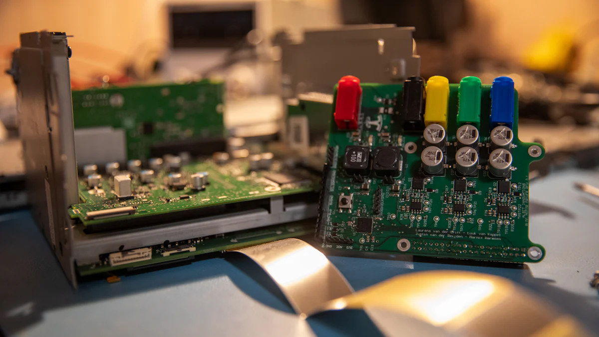
DIPs come in various types, each tailored for specific applications. General-purpose integrated circuits (ICs) are the most common, offering versatility for a wide range of uses. Microcontrollers, operational amplifiers, and memory chips frequently utilize this package. These components play vital roles in data processing, communication systems, and control mechanisms.
The adaptability of DIPs extends to both simple and complex circuits. Hobbyists often use them for basic projects due to their ease of assembly. Professionals rely on them for prototyping advanced systems, where durability and replaceability are critical. The package's compatibility with sockets further enhances its usability, allowing for quick replacements during testing or repairs.
"The DIP package's layout is well-suited for a range of applications, from basic circuits to more complex systems, providing a stable and reliable connection within the electronic device."
This versatility ensures that DIPs remain relevant in educational settings and legacy systems, despite the rise of surface-mount technology. Their continued use fosters innovation and provides a reliable foundation for learning and experimentation.
How to Use a Dual In-line Package in Your Projects
Handling and Preparing DIPs
Proper handling of a Dual in-line package ensures its functionality and longevity. Users should always work in an anti-static environment to prevent electrostatic discharge, which can damage sensitive components. Anti-static wrist straps or mats provide an effective solution for maintaining a safe workspace. When inserting the DIP into a circuit board or socket, precision tools like tweezers help avoid bending or damaging the pins.
Before installation, users should inspect the pins for alignment. Bent pins can disrupt the connection and compromise the circuit's performance. Straightening misaligned pins with care ensures a secure fit into the predesigned footprint. For projects requiring frequent component changes, using DIP sockets is highly recommended. These sockets allow easy insertion and removal without risking damage to the package or the circuit board.
"To properly handle a DIP package component, general rules include the use of an anti-static environment setup and proper tweezers for insertion into the predesigned footprint."
Soldering DIPs to Circuit Boards
Soldering a Dual in-line package to a circuit board requires precision and adherence to best practices. Begin by placing the DIP into the designated through-holes on the PCB. Ensure the pins align correctly with the holes to avoid misconnection. Once positioned, secure the component temporarily with tape or a fixture to prevent movement during soldering.
Use a soldering iron with a temperature-controlled tip to avoid overheating the DIP. Excessive heat can damage the package or the PCB. Apply solder to each pin individually, ensuring a clean and solid connection. Avoid using excessive solder, as it may create bridges between adjacent pins, leading to short circuits. After soldering, inspect the joints for consistency and test the connections with a multimeter to confirm proper functionality.
"Soldering should use proper techniques and temperatures to avoid damaging the package."
Integrating DIPs into Circuits
Integrating a Dual in-line package into a circuit involves understanding its pin configuration and ensuring compatibility with the design. Referencing the datasheet of the specific DIP component provides essential details about pin functions and electrical characteristics. This step minimizes errors during integration.
When connecting the DIP to other components, use jumper wires or traces on the PCB to establish the required connections. Verify the orientation of the DIP by locating the notch or dot that indicates the first pin. Incorrect orientation can lead to circuit failure or component damage. Testing the circuit on a breadboard before final assembly ensures that the DIP functions as intended and reduces the risk of errors during soldering.
The versatility of DIPs makes them suitable for various applications, from simple educational projects to complex prototypes. Their compatibility with breadboards and sockets simplifies the integration process, allowing users to experiment and refine their designs with ease.
Reading Datasheets for DIPs
Reading datasheets is a critical step when working with a Dual in-line package. These documents provide essential information about the component's specifications, pin configurations, and electrical characteristics. Understanding this data ensures proper integration into circuits and prevents potential errors during assembly.
Datasheets typically include a detailed pinout diagram. This diagram identifies each pin's function, such as power supply, ground, or signal input/output. Users should carefully study this section to avoid incorrect connections. For instance, connecting a power pin to the wrong voltage source can damage the component permanently. The datasheet also highlights the orientation marker, usually a notch or dot, which helps identify the first pin.
Electrical parameters, such as voltage ratings, current limits, and operating temperature ranges, are also outlined in the datasheet. Adhering to these specifications ensures the DIP operates reliably within its designed limits. Exceeding these parameters can lead to overheating, malfunction, or even failure of the component. Users should match these values with their circuit requirements to maintain compatibility.
Datasheets often include recommended soldering guidelines. These guidelines specify the maximum soldering temperature and duration to prevent damage to the package. For example, experts in PCB assembly emphasize the importance of using proper soldering techniques and controlled temperatures to protect the DIP during installation. Following these recommendations ensures a secure and durable connection.
Additionally, datasheets may provide application notes or example circuits. These examples demonstrate how to use the DIP effectively in various scenarios. Beginners can benefit from these practical insights, as they simplify the learning process and reduce trial-and-error efforts. Advanced users can reference these examples to optimize their designs.
"To properly handle a DIP package component, general rules include the use of anti-static environment setup and the use of proper tweezers in order to insert the component into the predesigned footprint."
By thoroughly reviewing the datasheet, users gain a comprehensive understanding of the Dual in-line package. This knowledge enhances their ability to design efficient circuits, troubleshoot issues, and maximize the component's performance.
Common Mistakes When Using Dual In-line Packages and How to Avoid Them
Incorrect Pin Alignment
Incorrect pin alignment often leads to circuit malfunctions or permanent damage to components. Users must ensure that the pins of the Dual in-line package align perfectly with the designated holes on the printed circuit board (PCB) or breadboard. Misalignment can result in improper connections, causing short circuits or open circuits.
To avoid this issue, users should inspect the orientation marker on the package, such as a notch or dot, which indicates the first pin. This marker helps identify the correct alignment. Before inserting the component, users should verify the pin configuration by referencing the datasheet. Straightening bent pins with precision tools ensures a proper fit. Testing the alignment on a breadboard before soldering provides an additional layer of assurance.
"Proper alignment of DIP pins is critical to prevent electrical failures and ensure reliable circuit performance."
Overheating During Soldering
Excessive heat during soldering can damage the Dual in-line package and compromise its functionality. High temperatures may cause the plastic housing to melt or the internal circuitry to fail. Overheating also risks damaging the PCB, leading to delamination or burnt traces.
To prevent overheating, users should employ a temperature-controlled soldering iron. Setting the temperature within the recommended range, typically between 300°C and 350°C, minimizes the risk of damage. Applying solder quickly and efficiently to each pin reduces heat exposure. Using heat sinks or clips on the pins can further protect the component during soldering. After soldering, inspecting the joints for consistency ensures a secure connection without excessive solder.
"Controlled soldering techniques safeguard both the DIP and the PCB from thermal damage."
Skipping Testing Before Soldering
Skipping the testing phase before soldering often results in costly errors and time-consuming rework. Without prior testing, users may overlook issues such as incorrect pin connections, faulty components, or design flaws. Once soldered, reversing these mistakes becomes challenging.
Testing the circuit on a breadboard allows users to identify and resolve potential problems before final assembly. This step ensures that the Dual in-line package functions as intended within the circuit. Verifying the pin configuration and electrical characteristics using a multimeter or oscilloscope enhances accuracy. Reviewing the datasheet for compatibility with the circuit design further reduces the likelihood of errors.
"Testing before soldering saves time and ensures the reliability of the final assembly."
By addressing these common mistakes, users can enhance the reliability and performance of their electronic projects. Proper alignment, controlled soldering, and thorough testing are essential practices when working with Dual in-line packages.
Pro Tips for Working with Dual In-line Packages
Using Sockets for Easy Replacement
Sockets provide a practical solution for working with a Dual in-line package. These components allow users to insert and remove DIPs without soldering, which simplifies the process of testing and replacing parts. Sockets also protect the pins of the DIP from wear and tear, ensuring the component remains functional over time.
To use sockets effectively, users should select the correct size and type for their DIP. Precision during installation is essential. The socket must align perfectly with the PCB holes to ensure a secure connection. After soldering the socket to the board, users can insert the DIP into the socket, ensuring proper orientation by referencing the notch or dot on the package. This approach minimizes the risk of damage during experimentation or repairs.
"Sockets enhance the versatility of DIPs, making them ideal for prototyping and educational projects where frequent adjustments are necessary."
Testing Circuits Before Soldering
Testing circuits before soldering ensures the reliability of the final assembly. Breadboards offer an excellent platform for this purpose, as they allow users to connect components temporarily without permanent modifications. By assembling the circuit on a breadboard, users can verify the functionality of the Dual in-line package and other components.
During testing, users should pay close attention to the pin configuration and electrical characteristics of the DIP. A multimeter or oscilloscope can help confirm proper connections and signal integrity. Any issues identified during this phase can be resolved before soldering, saving time and effort. Testing also provides an opportunity to optimize the circuit design, ensuring compatibility and performance.
"Breadboards and testing tools play a crucial role in identifying potential issues before committing to soldering."
Organizing and Storing DIPs
Proper organization and storage of Dual in-line packages extend their lifespan and maintain their usability. DIPs are sensitive to environmental factors such as moisture, dust, and static electricity. Storing them in anti-static containers or bags prevents electrostatic discharge, which can damage the components. Labeling each container with the component's specifications simplifies identification and retrieval.
For long-term storage, users should keep DIPs in a dry and temperature-controlled environment. Moisture-absorbing packets can be added to storage containers to protect against humidity. Organizing DIPs by type, size, or application ensures quick access during projects. This practice not only saves time but also reduces the risk of misplacing or damaging components.
"Effective storage solutions preserve the quality of DIPs and streamline the workflow for electronic projects."
By following these pro tips, users can maximize the efficiency and reliability of their work with Dual in-line packages. Sockets simplify replacements, testing prevents errors, and proper storage ensures the longevity of components. These practices contribute to successful electronic projects and foster a deeper understanding of circuit design.
The Dual in-line package remains a cornerstone in electronics due to its simplicity, versatility, and reliability. Its structured design, ease of integration, and compatibility with breadboards make it an essential tool for both beginners and professionals. By practicing with DIPs in small projects, users can build confidence and refine their skills. Over time, exploring advanced techniques and applications will unlock the full potential of these components. Whether for prototyping, learning, or innovation, DIPs continue to empower users to create efficient and high-quality electronic designs.
See Also
Maximizing Opportunities in High-tech Zones for Expansion
Mobile Smart Device Manufacturing Hub: Reach EVE Energy Effortlessly
Zhongkai's Transformative Approach to High-Energy Batteries
Zhongkai High-tech Zone: Center for Smart Device Advancements
Huizhou Zhongkai High-tech Zone: Fostering Innovation in Electronics

Zhongkai High tech Zone National foreign trade transformation and Upgradi Base(Electronic Information)Cloud Platform.
Address: Zhongkai High-tech Zone,Huizhou City ,Guangdong,China
E-mail: huizhoueii@163.com 13510001271@163.com
Tel: +86-0752-3279220 Mobile: +86-13510001271